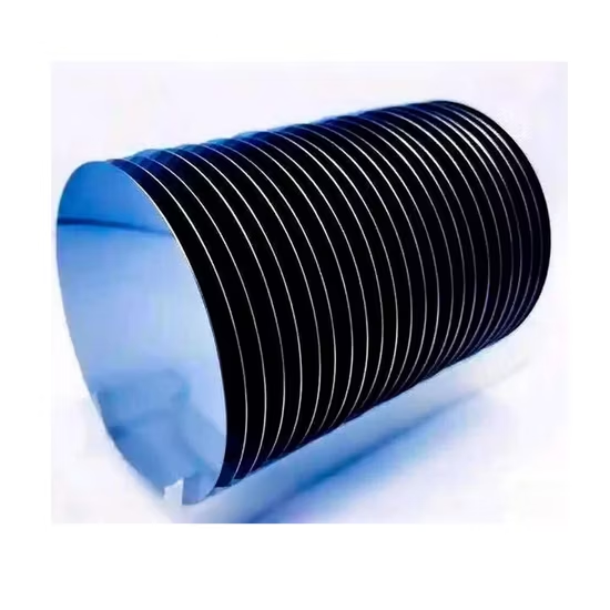
The demand for high-performance semiconductor materials has grown rapidly with the advancement of renewable energy, consumer electronics, electric vehicles, and industrial automation. Among the most important materials in these industries are n-type monocrystalline silicon wafers. These wafers are known for their excellent electrical conductivity, high purity, and superior efficiency, making them the preferred choice for advanced solar cells and semiconductor devices.
Unlike conventional silicon wafers, n-type monocrystalline silicon wafers offer improved carrier lifetime, reduced degradation, and better overall performance. They are widely used in the production of photovoltaic (PV) solar panels, integrated circuits, sensors, and power electronics. Whether you are a manufacturer, engineer, researcher, or technology enthusiast, understanding the characteristics and applications of these wafers is essential.
This article provides a detailed overview of n-type monocrystalline silicon wafers, including their manufacturing process, benefits, applications, technical specifications, and tips for selecting a reliable supplier.
Table of Contents
- What Are N-Type Monocrystalline Silicon Wafers?
- Manufacturing Process of N-Type Monocrystalline Silicon Wafers
- Key Features of N-Type Monocrystalline Silicon Wafers
- Advantages of N-Type Monocrystalline Silicon Wafers
- Applications Across Different Industries
- N-Type vs. P-Type Silicon Wafers
- Important Technical Specifications
- Quality Standards and Testing
- How to Choose the Right Supplier
- Future Trends in N-Type Silicon Technology
- Frequently Asked Questions
- Conclusion
What Are N-Type Monocrystalline Silicon Wafers?
N-type monocrystalline silicon wafers are ultra-pure slices of single-crystal silicon that are doped with donor elements such as phosphorus. The added phosphorus atoms provide extra electrons, making electrons the primary charge carriers within the material.
Because these wafers are made from a single crystal, they have a highly uniform atomic structure with very few defects. This results in excellent electrical performance and higher efficiency compared to many other silicon materials.
They are commonly used in:
- Solar photovoltaic cells
- Semiconductor chips
- Power electronics
- MEMS devices
- Microprocessors
- Sensors
- Integrated circuits
- Research laboratories
Their superior performance has made them a preferred material in many advanced manufacturing industries.
Manufacturing Process of N-Type Monocrystalline Silicon Wafers
Producing n-type monocrystalline silicon wafers requires sophisticated manufacturing techniques and strict quality control.
Silicon Purification
The process begins with refining raw silicon into electronic-grade silicon with extremely high purity levels.
Crystal Growth
Manufacturers use methods such as the Czochralski (CZ) process or Float Zone (FZ) process to grow a single-crystal silicon ingot.
Doping Process
Phosphorus or another donor material is introduced during crystal growth to create n-type conductivity.
Ingot Shaping
The silicon ingot is ground into a uniform cylindrical shape suitable for wafer slicing.
Precision Slicing
Diamond wire saws cut the ingot into thin wafers with highly accurate thickness.
Surface Polishing
Chemical-mechanical polishing creates an extremely smooth surface that meets semiconductor manufacturing standards.
Final Inspection
Each wafer undergoes comprehensive testing to verify thickness, resistivity, flatness, crystal orientation, and surface quality.
Key Features of N-Type Monocrystalline Silicon Wafers
Several characteristics distinguish n-type monocrystalline silicon wafers from other semiconductor materials.
High Purity
The silicon contains extremely low impurity levels, ensuring reliable electrical performance.
Uniform Crystal Structure
The continuous crystal lattice minimizes grain boundaries and electrical losses.
High Carrier Lifetime
Long electron carrier lifetime improves efficiency in both solar cells and electronic devices.
Excellent Thermal Stability
These wafers perform consistently across a wide range of operating temperatures.
Superior Mechanical Strength
Strong crystal integrity reduces the risk of cracking during manufacturing.
Low Defect Density
Minimal crystal defects improve production yields and device reliability.
Advantages of N-Type Monocrystalline Silicon Wafers
There are numerous reasons manufacturers increasingly choose n-type monocrystalline silicon wafers.
Higher Conversion Efficiency
Solar cells built with n-type wafers typically produce higher energy conversion efficiency.
Reduced Light-Induced Degradation
Unlike many p-type wafers, n-type silicon experiences significantly less performance loss over time.
Longer Product Lifespan
Lower impurity levels contribute to greater durability and extended service life.
Improved Electrical Conductivity
Electron mobility is higher, supporting better overall device performance.
Better Manufacturing Performance
Consistent crystal quality leads to higher production yields and fewer rejected components.
Enhanced Reliability
These wafers maintain stable performance throughout long operating periods.
Applications Across Different Industries
The versatility of n-type monocrystalline silicon wafers makes them suitable for numerous advanced technologies.
Solar Energy
High-efficiency photovoltaic modules rely on n-type wafers to maximize electricity production.
Semiconductor Manufacturing
Integrated circuits, processors, and memory devices are built using high-quality silicon wafers.
Power Electronics
Power conversion equipment benefits from the excellent conductivity of n-type silicon.
MEMS Technology
Micro-electromechanical systems require highly precise silicon substrates.
Optical Components
Some photonic devices use monocrystalline silicon because of its exceptional material properties.
Scientific Research
Universities and research laboratories frequently use these wafers for advanced semiconductor studies.
N-Type vs. P-Type Silicon Wafers
Understanding the differences helps manufacturers choose the correct material.
| Feature | N-Type Silicon | P-Type Silicon |
| Dopant | Phosphorus | Boron |
| Primary Carrier | Electrons | Holes |
| Light-Induced Degradation | Very Low | Higher |
| Solar Efficiency | Higher | Moderate |
| Carrier Lifetime | Longer | Shorter |
| Material Cost | Higher | Lower |
Although p-type wafers remain common, n-type monocrystalline silicon wafers are increasingly preferred for premium applications where maximum efficiency is required.
Important Technical Specifications
When purchasing n-type monocrystalline silicon wafers, evaluate the following specifications.
Wafer Diameter
Common sizes include:
- 100 mm
- 150 mm
- 200 mm
- 300 mm
Thickness
Thickness varies according to semiconductor or photovoltaic manufacturing requirements.
Resistivity
Different applications require different resistivity values depending on electrical performance.
Crystal Orientation
Typical crystal orientations include:
- <100>
- <111>
Surface Finish
Manufacturers offer:
- Single-side polished
- Double-side polished
- Lapped
- Epitaxial-ready surfaces
Flatness
Excellent flatness is essential for accurate photolithography and semiconductor fabrication.
Quality Standards and Testing
Leading manufacturers perform extensive inspections before shipping n-type monocrystalline silicon wafers.
Common quality tests include:
- Surface defect inspection
- Thickness measurement
- Flatness analysis
- Resistivity testing
- Crystal orientation verification
- Particle contamination inspection
- Mechanical strength evaluation
- Optical surface examination
Strict quality control ensures consistent manufacturing performance.
How to Choose the Right Supplier
Choosing a reliable supplier is essential for obtaining premium n-type monocrystalline silicon wafers.
Manufacturing Experience
Select suppliers with proven expertise in semiconductor-grade silicon production.
International Certifications
Look for manufacturers that follow recognized quality management standards.
Custom Manufacturing
Many applications require custom diameters, resistivity ranges, or surface finishes.
Technical Support
Experienced engineering teams can assist with selecting appropriate wafer specifications.
Reliable Production Capacity
Consistent manufacturing processes ensure dependable quality across large orders.
Delivery Performance
Reliable logistics help maintain uninterrupted production schedules.
Future Trends in N-Type Silicon Technology
The future of n-type monocrystalline silicon wafers remains highly promising.
Emerging developments include:
- TOPCon solar cell technology
- Heterojunction solar cells
- Thinner silicon wafers
- Improved crystal growth methods
- Higher photovoltaic efficiency
- Lower manufacturing costs
- Expanded use in electric vehicles
- Advanced semiconductor fabrication
As renewable energy and electronics continue to evolve, n-type silicon technology will remain at the forefront of innovation.
Frequently Asked Questions
What are n-type monocrystalline silicon wafers?
They are single-crystal silicon wafers doped with phosphorus or similar donor elements to create electron-based conductivity.
Why are they preferred for solar cells?
They provide higher efficiency, lower degradation, and longer operational life compared to many traditional silicon wafers.
Which industries use these wafers?
They are widely used in solar energy, semiconductor manufacturing, MEMS devices, integrated circuits, power electronics, and scientific research.
What crystal orientations are available?
The most common orientations are <100> and <111>, depending on manufacturing requirements.
Are n-type wafers more expensive?
Yes. Their advanced manufacturing process and higher performance generally result in a higher price than p-type wafers.
What should I consider when selecting a supplier?
Evaluate product quality, manufacturing experience, technical support, certifications, customization capabilities, and delivery reliability.
Conclusion
N-type monocrystalline silicon wafers are among the most advanced semiconductor materials available today. Their exceptional purity, superior carrier lifetime, high electrical conductivity, and excellent long-term reliability make them the preferred choice for modern solar panels, integrated circuits, power electronics, and research applications. As industries continue to demand higher efficiency and greater performance, these wafers will remain a key component in next-generation technologies. By working with a trusted supplier and selecting the right technical specifications, manufacturers can improve production quality, reduce defects, and build innovative products that meet the growing needs of the global technology market.